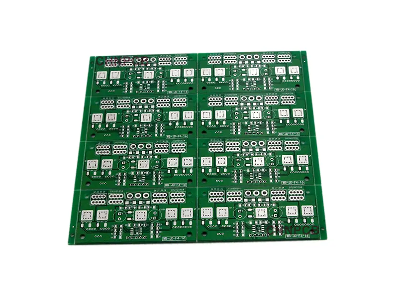

For new PCB engineers, manually creating a component footprint in Altium Designer (AD) is one of the most important foundational skills. A correctly drawn footprint ensures your components will fit perfectly on the finished board. This guide walks through every step with clear instructions and screenshots so you can follow along directly in your own AD workspace.
Before You Start: What You Need:
Before drawing a footprint, always download the component datasheet from the manufacturer's website. The datasheet contains:
Exact pad dimensions and spacing
Component body size
Drill hole diameter for through-hole components
Recommended land pattern
Never draw a footprint from memory. One millimeter of error can make an entire batch of boards unusable.

Step 1: Create a New PCB Library File
Open Altium Designer. In the top menu, click:
1.File → New → Library → PCB Library
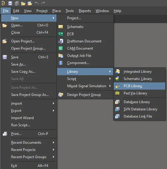
2.A blank .PcbLib workspace opens automatically.
3.Save the file immediately using Ctrl + S. Name it something meaningful, such as MyProject_Components.PcbLib.
Step 2: Rename the Footprint
In the PCB Library panel on the left side, you will see a default footprint named "PCBComponent_1".
Double-click on the name to rename it. Use a clear naming format, for example:
Through-hole resistor: RES_AXIAL_2.54mm
SMD capacitor: CAP_0805
IC chip: DIP-8_2.54mm
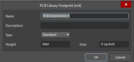
Rename
Step 3: Set the Grid and Units
Press G to open the Grid Manager.
Set the grid pitch to match your component's pad spacing:
Through-hole components: 2.54mm (100mil)
SMD components (0805, 0603): 0.5mm or 0.25mm
Fine-pitch IC: 0.1mm
Press Q at any time to toggle between mm and mil units.
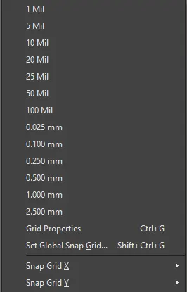
Switching units between mil and mm in Altium Designer for PCB grid accuracy
Step 4: Place the First Pad
Press P → P to activate the pad placement tool. Before clicking to place, press Tab to open the Pad Properties dialog.
For a through-hole component (example: 2-pin resistor), set:
Designator: 1
Shape: Round
Hole Size: 0.8mm
X Size / Y Size: 1.6mm / 1.6mm
Layer: Multi-Layer

Click OK, then click at the origin point (0,0) to place Pad 1.
Once all pads are placed, continue with the following steps to complete your footprint with silkscreen, courtyard, and reference designator.
Step 5: Place the Remaining Pads
For a 2-pin through-hole resistor with 2.54mm pitch, place Pad 2 at coordinates (2.54, 0).
To enter exact coordinates while placing:
Press J → L to open the Jump to Location dialog, enter the X and Y coordinates, then place the pad.
For components with more pins (DIP-8, DIP-16, etc.), repeat this process for each pin, referencing the datasheet pin spacing exactly.
Step 6: Draw the Silkscreen Outline
Switch to the Top Overlay layer by clicking the layer tab at the bottom of the workspace, or press the layer shortcut key.
Go to Place → Line (or press P → L) and draw a rectangle around the component body outline as specified in the datasheet.
Important rules for silkscreen:
Do not draw over pads
Keep lines at least 0.1mm away from pad edges
Use 0.2mm line width as standard
Step 7: Draw the Courtyard Boundary
Switch to the Courtyard_Top layer.
Use Place → Line to draw a rectangle that surrounds the entire component including the silkscreen outline, with at least 0.25mm clearance on all sides.
The courtyard tells Altium Designer's Design Rule Check (DRC) where the component boundary is, preventing components from being placed too close together during layout.
Step 8: Add the Component Reference Point
Go to Place → String and place the .Designator string on the Top Overlay layer, positioned above the component outline.
This reference designator (R1, C1, U1, etc.) will appear on the finished board silkscreen, helping the assembly team identify each component.
Step 9: Run the Footprint Wizard Check and Save
Before saving, do a quick visual check:
All pads numbered correctly
Silkscreen does not overlap pads
Courtyard completely surrounds the component
Dimensions match the datasheet
Step 10: Link the Footprint to Your Schematic Component
Open your schematic library (.SchLib). Select the component symbol you want to link. (
In the Properties panel on the right, find the Footprint section and click Add.
Browse to your .PcbLib file, select the footprint you just created, and click OK.
Save the schematic library. Your footprint is now ready to use.
Guangzhou Mineng Electronics Co., Ltd. (CHNPCB) is a PCB manufacturer based in Guangzhou's Baiyun District, serving engineers and procurement teams across the Greater Bay Area and international markets. Founded in 2015, CHNPCB specializes in single-sided PCBs, double-sided PCBs, and aluminum substrate boards, with production capabilities covering standard FR-4, heavy copper, and extra-long board formats up to 1200mm.
All standard double-sided PCBs are produced using Kingboard KB6160 copper-clad laminate, a UL-certified material that delivers consistent electrical performance and thermal stability — ensuring that the footprints you carefully designed in Altium Designer translate into a reliable, manufacturable board.