

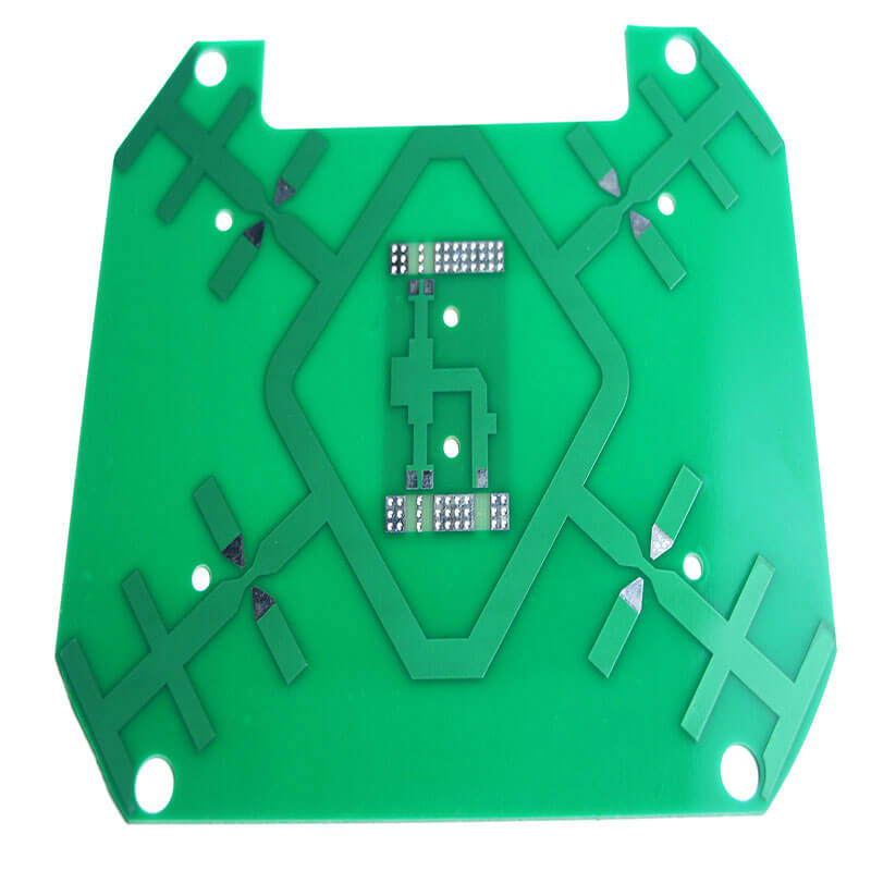
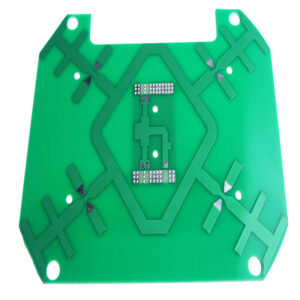
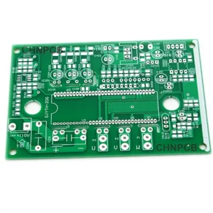
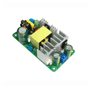
Description
Our 2 Layer PCB, also known as a double-sided printed circuit board, is a cost-effective and reliable solution for a wide range of electronic applications. Featuring copper layers on both sides of the substrate, it allows for higher routing density and stable electrical performance compared to single-sided boards. Electrical connections between layers are made using plated through holes (PTH), ensuring consistent signal integrity and durability.
We use high-quality FR-4 materials such as NanYa (Nanya) or KB6160, both of which are globally recognized for their excellent dielectric properties, thermal stability, and mechanical strength. These materials ensure the 2 Layer PCB performs reliably under different operating conditions and is suitable for both prototyping and mass production.
Key Features
- Double-sided . copper layers for efficient circuit routing
- Reliable plated through-hole (PTH) interconnection
- Stable FR-4 materials (NanYa / KB6160)
- Good thermal resistance and electrical insulation
- Cost-effective for both prototyping and volume production
-
Technical Specifications
Item Specification Layer Count 2 Layers Base Material FR-4 (NanYa / KB6160) Board Thickness 0.6mm – 2.0mm Copper Thickness 1oz – 2oz Min Trace / Space 0.1mm / 0.1mm Min Hole Size 0.2mm Surface Finish HASL, Lead-Free HASL, ENIG, OSP Solder Mask Green / Red / Blue / Black / White Silkscreen White / Black
Material Advantage (NanYa / KB6160)
- Stable Supply: Widely used mainstream PCB laminate brands
- Reliable Performance: Consistent Tg and dielectric properties
- Good Process Compatibility: Suitable for drilling, plating, and soldering
- Cost vs Performance Balance: Ideal for standard 2-layer PCB applications
Manufacturing Capabilities
-
- Precision CNC drilling and high-resolution imaging for accurate circuit patterns
- Automated etching and plating processes for consistent quality
- AOI (Automated Optical Inspection) to detect pattern defects
- X-RAY inspection to ensure via and solder joint reliability
- 100% electrical testing to guarantee functionality before shipment
- Flexible production, supporting both small batches and large volume orders
-
Applications
- Power supply boards
- LED lighting modules
- Consumer electronics
- Industrial control systems
- Automotive electronics (general applications)
-
Why Choose Us
- One-stop service: PCB + SMT + assembly
- Fast prototype lead time (24 hours available)
- Strict quality control based on IPC standards
- Flexible production capacity (prototype to mass production)
- Experience with global OEM/ODM customers
Company Information
Guangzhou MingEn Electronics Co., Ltd. specializes in PCB and PCBA manufacturing with stable quality and fast delivery. Our 2 Layer PCBs are built using reliable materials such as NanYa and KB6160, ensuring consistent performance for international customers.
For quotation and technical support, please contact us.
- Get a Quote
Looking for a reliable 2 Layer PCB supplier?
Send your requirements or Gerber files to: PCB@chnpcb.com
Our team will get back to you within 24 hours.
Reviews
There are no reviews yet.