

What Is a Resin Filled and Capped Via?
A via is a plated hole that connects copper layers. In a resin filled and capped via, the barrel is first plated with copper, then plugged with non-conductive epoxy resin, planarized flush with the board surface, and finally plated over with a copper cap. The via still conducts current and heat through its copper wall, but the surface above it becomes a flat, solid pad.
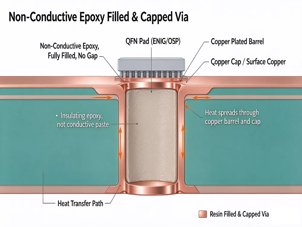
Schematic illustration of a non-conductive epoxy filled and capped via.
Why Fill Thermal Vias Under Pads
An open via placed inside a pad acts like a drain for molten solder. The consequences are familiar to anyone who has debugged a power board:
- Solder wicks into the barrel and leaves a starved joint
- Voids form under the thermal pad of QFN and power packages
- Trapped flux or air can cause uneven reflow
Filling and capping removes the drain, gives the assembler a flat surface, and keeps the thermal path through the copper barrel intact.
Resin Filled vs Conductive Filled vs Open Vias
| Via type | Surface flatness | Solder wicking | Relative cost | Typical use |
|---|---|---|---|---|
| Open or tented via | Not flat | Possible if under a pad | Low | Ordinary signal and power routing |
| Non-conductive resin filled and capped | Flat | Blocked | Medium | Via-in-pad, thermal pads, fine-pitch parts |
| Conductive paste filled | Flat | Blocked | High | Designs that need the fill itself to carry more current or heat |
CHNPCB uses non-conductive epoxy resin. Heat travels through the plated copper wall and the cap, which is the usual approach for thermal pad designs.
Resin Filled Vias PCB Design Limits at CHNPCB
These are the working limits for filled and capped vias:
- Minimum hole size: 0.15mm
- Board thickness range: 0.2-3.0mm
- Fill material: non-conductive epoxy resin
- Order size: prototypes and small batches
- Typical lead time: 15-20 days
The maximum thickness-to-hole ratio and the cap copper requirement depend on the stack-up, so the fastest route is to send the Gerber files and mark which vias need filling, with the drill size and quantity for each. As a pcb manufacturer that handles non-standard requests, we review these details case by case instead of rejecting anything outside a fixed menu.
Process Flow in Five Steps
- Drill the holes and plate the barrel with copper
- Plug the holes with non-conductive epoxy resin
- Cure the resin
- Grind the surface flush with the copper
- Plate the copper cap, then continue with outer layer processing and surface finish
Because the capped pads are flat, they suit finishes such as ENIG and OSP.
Common Defects and How to Prevent Them
Typical problems include voids inside the resin, dimples on the cap surface, and cap cracking or delamination after reflow. Controlling the cure, keeping the planarization even, and checking cross-sections on prototype lots are the usual ways to catch them early.
Where Filled Thermal Vias Are Used
Filled and capped vias appear on power supply boards, battery charging boards, LED lighting boards, and communication or control boards that use QFN, BGA, or power packages. For very high heat loads, a metal-core option such as an aluminum PCB may be a better route than a via array alone.
Custom Resin Filled Via Requests at CHNPCB
As a PCB company from China, we review every filled via request against the board thickness and hole size before quoting, because those two numbers decide whether the process is practical.
Guangzhou Mingen Electronics Co., Ltd. (CHNPCB) supports resin filled vias PCB orders from prototype to small batch for customers in Hong Kong,Taiwan,Singapore, Australia, and Europe, with a typical lead time of 15-20 days. To check your design, contact us with your Gerber files and the list of vias to fill at PCB@CHNPCB.COM.